Intro
Although the standards for 5G have not been finalized yet, general expectations for this fifth generation of mobile networks are high. 5G is expected to enable extreme mobile broadband with data rates up to 10Gbps, in order to meet, for example, the future demand for video streaming. It also promises to enable machine-to-machine communication in support of the Internet-of-Things Platform. And it is expected to allow for critical machine communication – such as driverless cars communicating with each other and with neighboring base stations. These applications typically require extremely high reliability, and low latencies, below 1ms.
To allow for this almost unlimited experience, innovations are required in the overall network infrastructure (including base stations and small cells) as well as in the technologies for mobile devices.
In the first phase of the 5G deployment, wireless communication radios will most probably operate in the sub-6GHz radio frequency (RF) bands. But to cope with the upcoming spectrum scarcity within these bands, bandwidth is being sought at millimeter-wave (mm-wave) bands – more specifically the RF bands within the 24 to 100GHz range. The introduction of these mm-wave frequencies will have a significant impact on the overall 5G network infrastructure. For mobile handsets such as smartphones, this translates into an increasing complexity of the RF front-end modules – that contain e.g. the transmitter/receiver, bandpass filters, power amplifiers and local oscillators. Both sub-6GHz bands and mm-wave bands will now need to be enabled in one common architecture, and devices will probably need to access several bands simultaneously. Therefore, higher speed front-end devices than currently used in 4G-LTE are needed. Also, the mm-wave functionality will have to be implemented in battery powered mobile devices, which will put severe restrictions on the power consumption of the mm-wave circuits. To meet all these challenges, we will need high-speed devices that have both a high output power and a high power efficiency.
Schematic representation of the increased RF-front-end-module complexity with every generation of mobile communication.
State-of-the-art high-speed devices
Today, several device technologies are being used for RF applications, including for example RF SOI and SiGe technologies. Of particular interest is the use of III-V circuits. III-V high electron mobility transistors (HEMTs, GaAs or InP based) are already in standard use for high-frequency applications. The RF performance of these devices significantly outperforms that of standard Si CMOS devices, especially when considering FinFETs which suffer from intrinsically higher parasitics. Next to that, III-V heterojunction bipolar transistors (HBTs) have also shown great potential when high speed requirements need to be fulfilled. And, although originally designed for high-power applications, III-N devices (such as GaN-based HEMT devices) have demonstrated high-frequency performance exceeding 400GHz.
So far, Si and III-V (or III-N) circuits have been fabricated and packaged separately, and then later assembled on the same carrier substrate. This approach however does not really allow for the optimization of the performance, the reduction of power, cost and form factor, and the increase in the complexity of the circuits. Reducing the form factor will however be essential, as many different dies will be needed to fabricate the RF front-end module, and space within the mobile handset is limited. The fabrication of III-V-based devices presents other challenges. In general, (lab-like) fabrication processes and materials are being used that are not compatible with cost-effective high-volume Si manufacturing. In addition, these III-V HEMT and HBT devices are mostly fabricated on smaller size (2 to 3 inch) non-Si substrates.
High-speed analog/RF: addressing the 5G performance needs for mobile devices
To enable RF front-end modules for future 5G mobile handsets, imec has launched the Industrial Affiliation Program ‘High-speed analog/RF’ – starting as from January 2018.
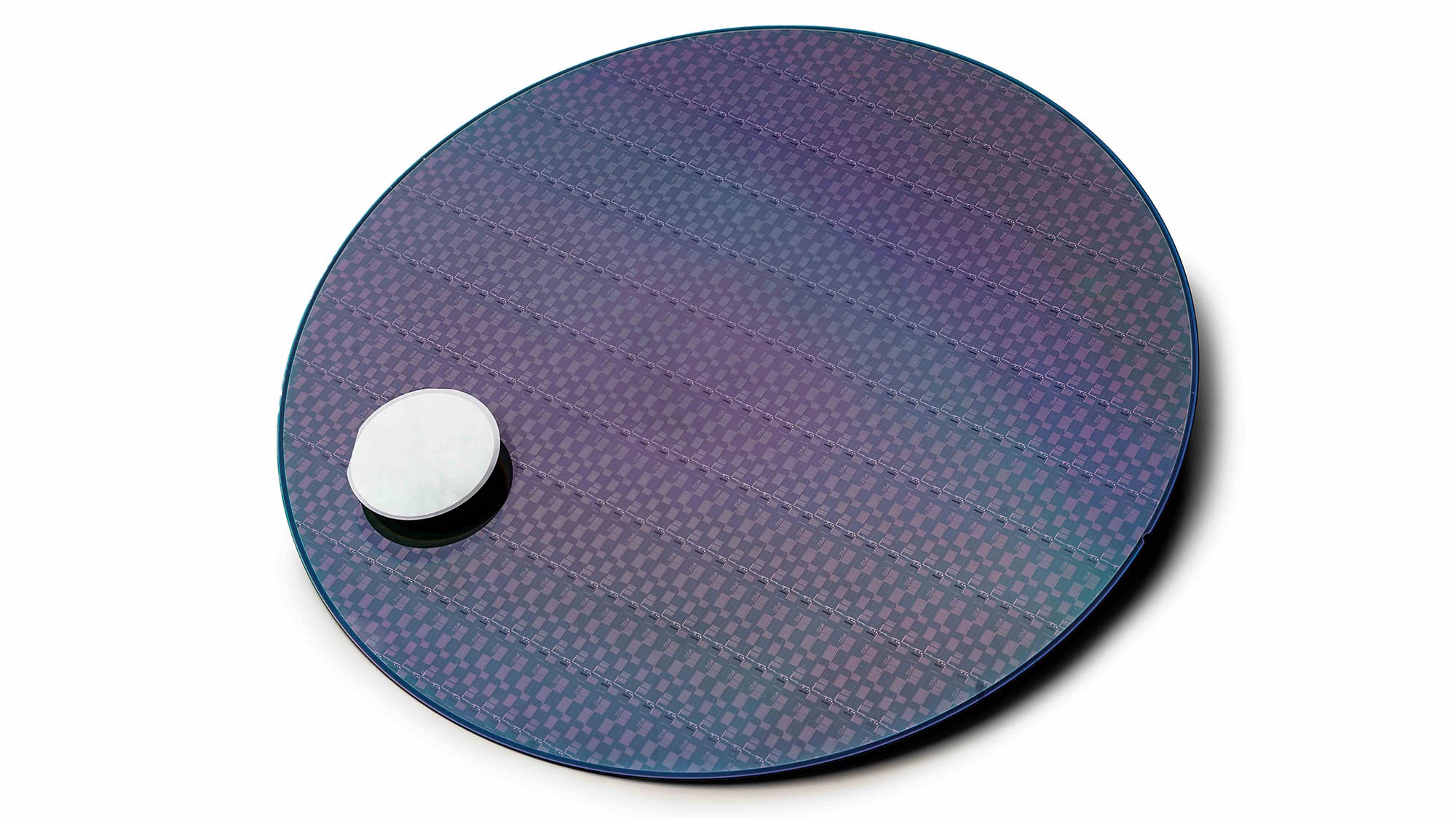
Within this program, imec and its partners will jointly explore hybrid Si/III-V to enable highly performant RF devices with high output power and high power efficiency.
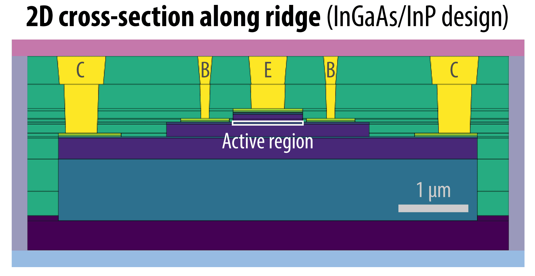
On the III-V side, imec will explore several device architectures, including III-V (GaAs and InP) and III-N HEMT devices, III-V HBT devices, as well as III-V and III-N MOSFET devices.
In a first phase, the program will focus on integrating III-V and III-N standalone devices on a 200mm and 300mm Si platform. This will require the development of specific process steps and modules that have been identified as critical for the integration. Examples are modules that reduce the parasitics in these non-Si devices; the epitaxial growth of RF-compatible III-V and III-N buffer layers (which are needed to compensate for the lattice mismatch between the III-V and III-N materials and Si); modules for gate stack optimization; and defectivity assessment. Also, the use of CMOS-compatible Cu or W based back-end-of-line processes will be investigated, to replace the Au-based interconnect schemes typically used for the non-Si devices. During this first phase, the program partners will also look into the scalability of the III-V and III-N devices. Making smaller III-V/III-N devices is currently challenged by the current-driven operation mode of the devices, and by the patterning technologies that are being used.
In a second phase, the program will target the co-integration of the specialized high-speed III-V/ III-N devices (used for the RF transceiver) with standard Si CMOS (used for the digital signal processing). This way, a higher degree of integration will be achieved for all building blocks of the RF front-end module. Imec sees two advantages of this co-integration. First, it will further reduce the overall form factor of the front-end module. And second, with the help of digitally assisted RF circuit design, hybrid Si/III-V technology can be seen as a way forward to improve the energy efficiency of the overall circuit. Several approaches for the co-integration will be explored, such as monolithic or 2D integration (with the Si devices and III-V/III-N devices in the same plane) or 3D integration (via either 3D stacking, or sequential 3D through the sequential processing of different device layers).
Leveraging existing technology solutions
Imec houses several key technologies under one roof and is therefore uniquely placed to develop hybrid Si/III-V RF front-end technologies for 5G applications.
For example, the program partners will make use of imec’s expertise on III-V-on-300mm Si technologies – developed in the context of CMOS scaling. More specifically, imec will bring in extensive knowledge of III-V technologies, including III-V epitaxial growth on Si, gate-stack and contact optimization, and reliability assessment. Imec can also rely on an extended CMOS toolset, such as 193nm (immersion) lithography and CMOS compatible back-end-of-line modules.
The analog/RF program will also leverage imec’s expertise in III-N technology, such as our GaN-on-200mm Si technology platform. Originally developed for power electronics applications, it will be investigated how these GaN-on-Si devices can be tuned towards RF applications. For example, the buffer layers will have to be made RF compatible, and the devices will have to be re-designed for lower operating voltages.
And we will use our expertise on sub-6GHz and mm-wave wireless communication technologies. Close collaboration with the modelling and circuit design teams will be essential to define the required device targets for 5G applications. Their work will be supported by the use of advanced circuit design techniques such as RF design and technology co-optimization (RF DTCO).
Bringing together expertise in III-V and III-N technology, CMOS technology, wireless communication technologies, and in modelling and circuit design technologies will be crucial to the development of true RF front-end technology solutions for 5G – from device to circuit level.
Example: reliable III-V gate stacks – a key module for III-V MOSFET integration
Besides HEMT and HBT devices, imec will explore III-V-based MOSFET devices for RF front-end applications. Interest in these devices comes from their lower gate leakage and favorable scalability.
The development of reliable III-V-based MOSFETs is however challenged by the formation of gate stacks with low interface and gate dielectric defects. Devices that have e.g. InGaAs as a channel material, most commonly use Al2O3 as a dielectric material within the gate stack. But the excessive interaction of channel charge carriers with oxide defects (present within the dielectric material or at the semiconductor-oxide interfaces) significantly impacts the overall device reliability. This interaction translates into trapping/de-trapping of the charge carriers by the oxide defects, and causes, for example, instability of the device threshold voltage, or frequency dispersion in the C-V characteristics.
Various manifestations of oxide traps in the electrical characteristics of InGaAs devices with high-k gate stacks: (a) frequency dispersion of MOS C-V characteristics; (b) Vth and SS instability; (c) gm instability in planar MOSFETs; (d) hysteresis of the ID-VG characteristic of a FinFET.
At the 2017 IEDM conference, imec gave an invited talk, reviewing recent studies on oxide defects in InGaAs gate stacks for MOSFETs. An overview was given on the recent understanding of charge trapping, and guidelines were presented for developing reliable III-V gate stacks. These insights will highly contribute to solving one of the major integration challenges of III-V MOSFET devices on a Si platform.
Within the study, various trap characterization techniques, such as positive bias temperature instability (PBTI) and defect capture-emission-time maps, were performed on a variety of InGaAs device test vehicles (including planar MOSFETs, FinFETs and nanowires). With these techniques, we can determine, for example, the shift in threshold voltage induced by charge trapping, the time-to-failure, the device ageing, and the accessible defect density in an oxide. We observed that the PBTI signatures are common for all device architectures, while scaling introduces additional challenges. It was also found that device aging is dominated by the slow traps (slow capture/emission times), while the shift in threshold voltage is mainly caused by fast traps (fast capture/emission times).
Alternative characterization techniques such as multifrequency C-V dispersion and hysteresis were used to determine the distribution of the oxide defect levels (above and below the conduction band of the InGaAs channel). This distribution of energy levels dictates the charge trapping transients in the Al2O3-based InGaAs gate stacks. From these measurements, we found a more favorable distribution of defect levels when using alternative dielectrics such as HfO2.
The presented characterization of oxide traps is a crucial step towards the demonstration of reliable III-V gate stacks.
As an example, we propose an alternative, sufficiently reliable gate stack by replacing Al2O3 with a novel inter-dielectric layer (developed by ASM), capped by a thin LaSiOx layer and HfO2.
Conclusion
The advent of 5G will not only bring great new opportunities but also new challenges for the technologies enabling this next-generation of mobile communications. Not only innovations in the overall network infrastructure will be needed, but also in the technologies for the mobile devices themselves. Imec’s program on High-speed analog/RF aims at providing the required RF front-end module technologies for mobile handsets operating at sub-6GHz and mm-wave frequencies. In a first phase, focus will be on integrating high-speed III-V and III-N standalone devices on a 200mm and 300mm Si platform. In a second phase, the program partners will jointly explore the co-integration of these device architectures with standard Si CMOS. The program leverages imec’s broad expertise in III-V-on-300mm Si technologies, III-N technology, CMOS technologies, wireless communication technologies, and in modelling and circuit design technologies. Imec invites companies – material and equipment suppliers, IDMs, foundries and system companies – to become partner of the program.

Nadine Collaert received an M.S. and Ph.D. degree in electrical engineering from the ESAT Department, KU Leuven, Belgium, in 1995 and 2000, respectively. Since then, she has been involved in the theory, design and technology of FinFET devices, emerging memory devices, transducers for biomedical applications and the integration and characterization of biocompatible materials (e.g. carbon-based materials). From 2012 until April 2016 she was program manager of the imec LOGIC program, focusing on high mobility channels, TFET and nanowires. Since April 2016 she has been a distinguished member of technical staff, responsible for the research on novel CMOS scaling approaches based on heterogeneous integration of new materials with Si and new material-enabled device and system approaches to increase functionality. She has authored or co-authored more than 300 papers in international journals and conference proceedings, and she holds more than 10 patents in the field of device design and process technology. She has been a member of the CDT committee of the IEDM conference and she is still a member of the Program Committees of the international conferences ESSDERC, ULIS/EUROSOI and VLSI Technology Symposium.
Published on:
1 February 2018


