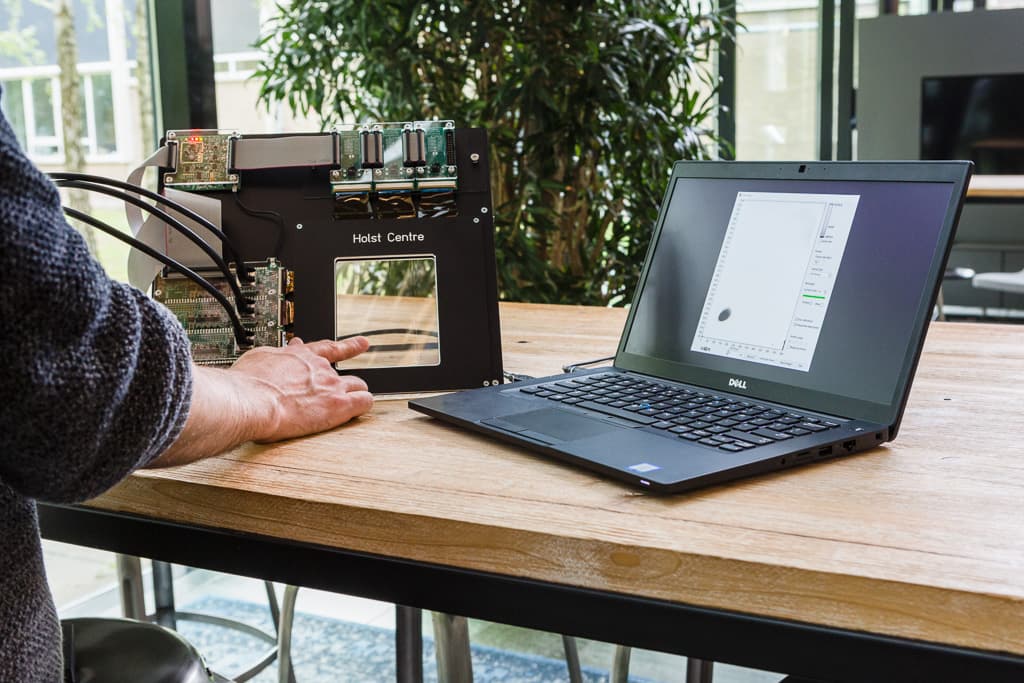
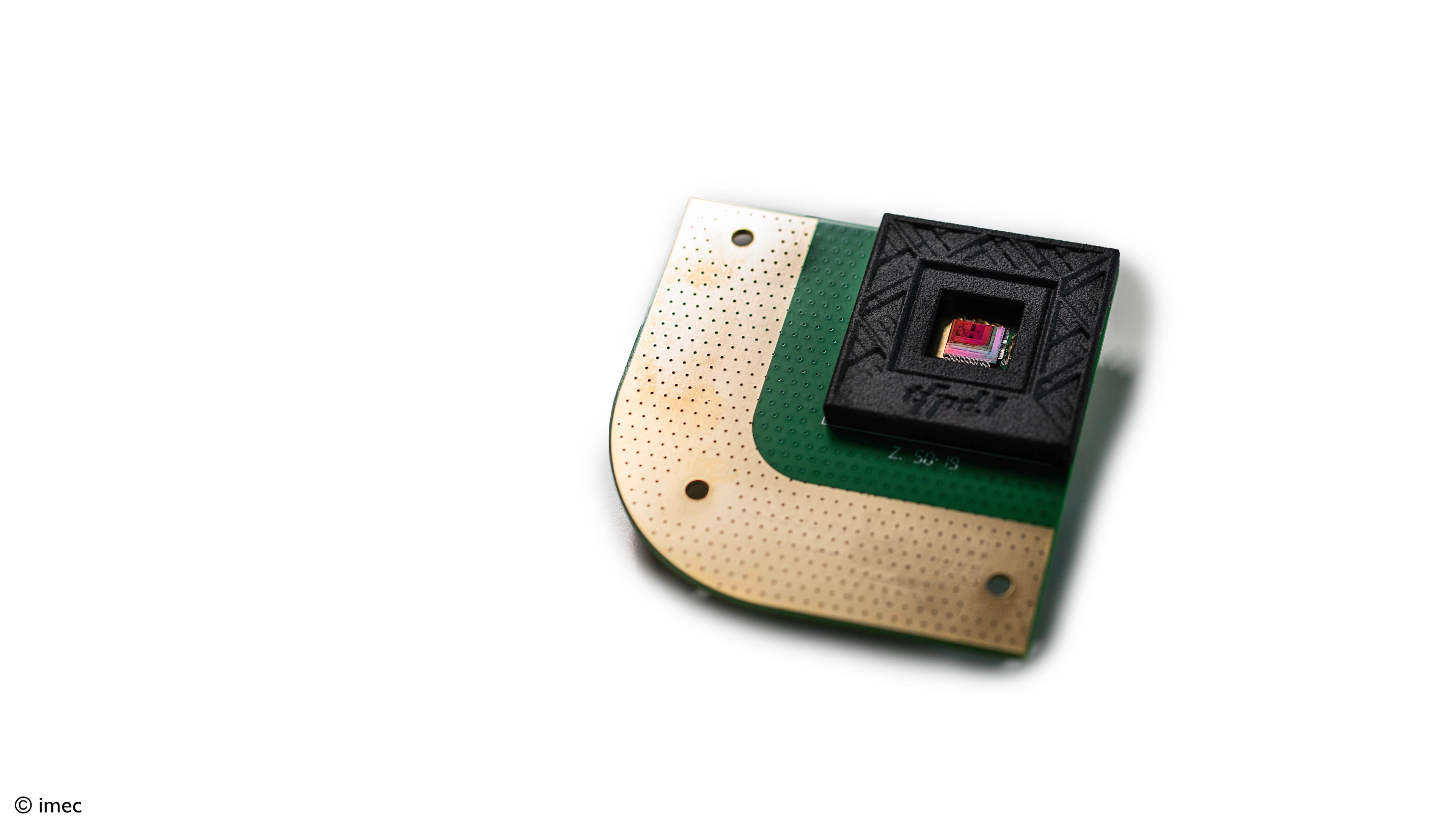
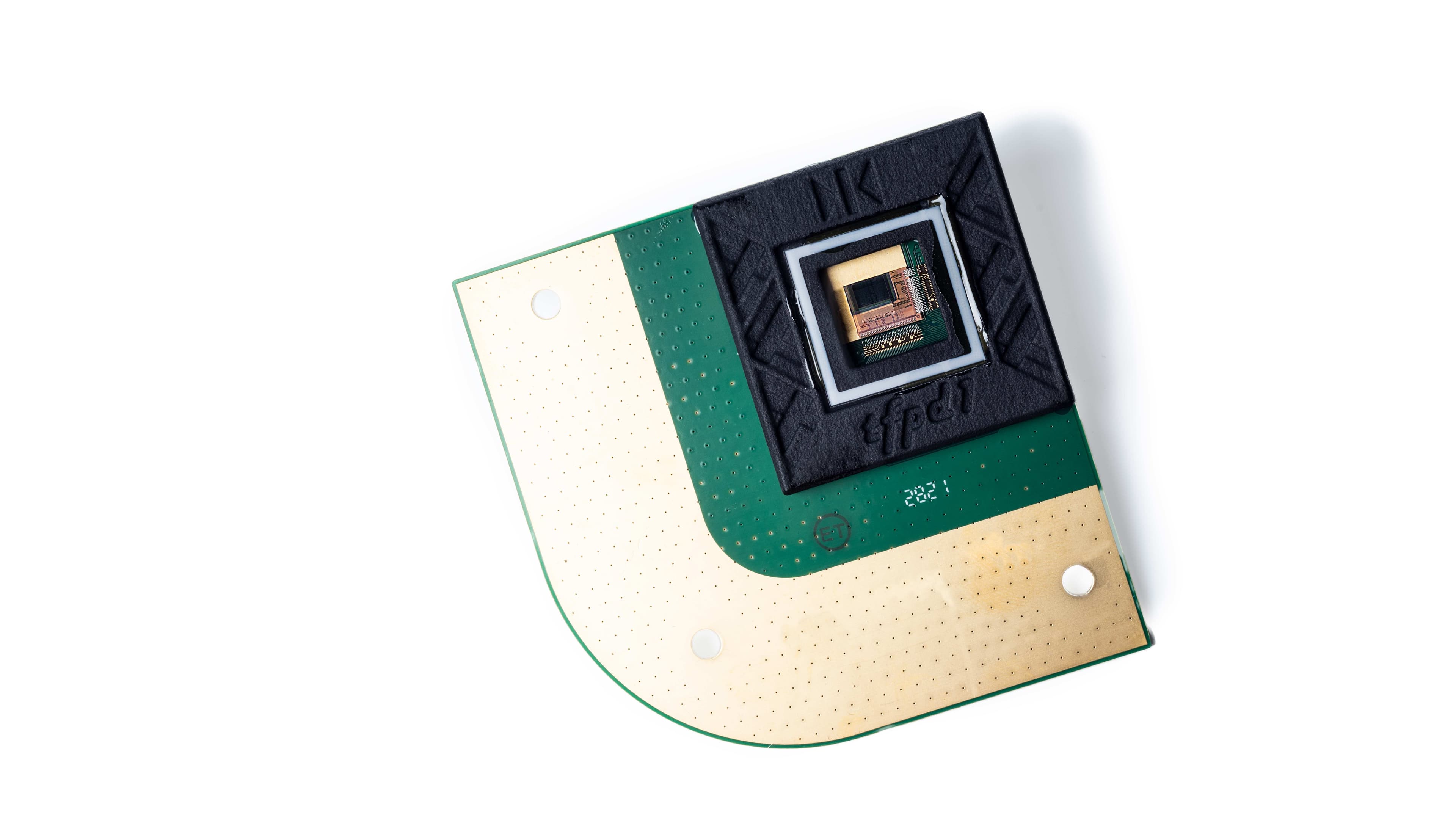
Could your car or an ATM recognize you just from your hand? Holst Centre, an open innovation initiative of imec and TNO, has developed a new large-area optical fingerprint sensor that is over 70% transparent – making it ideal for integrating on top of LCD displays. The new sensor will be publicly demonstrated for the first time at SID’s Display Week 2019 and could allow a wider range of display applications to incorporate biometric security.
The idea of integrating fingerprint scanners into displays is increasingly common in smartphones. These applications place a sensor under a transparent OLED array which acts as both the display and light source for the fingerprint reading. However, the LCD displays used, for example, in automotive applications, public transport systems and cash machines are more opaque and need a backlight, so are not suited to below-display fingerprint sensors. Instead, the sensor must be placed on top of the display which means it needs to be highly transparent so that the display can still be seen.
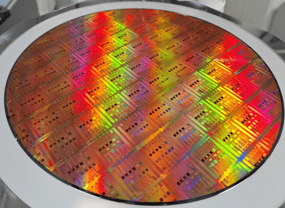
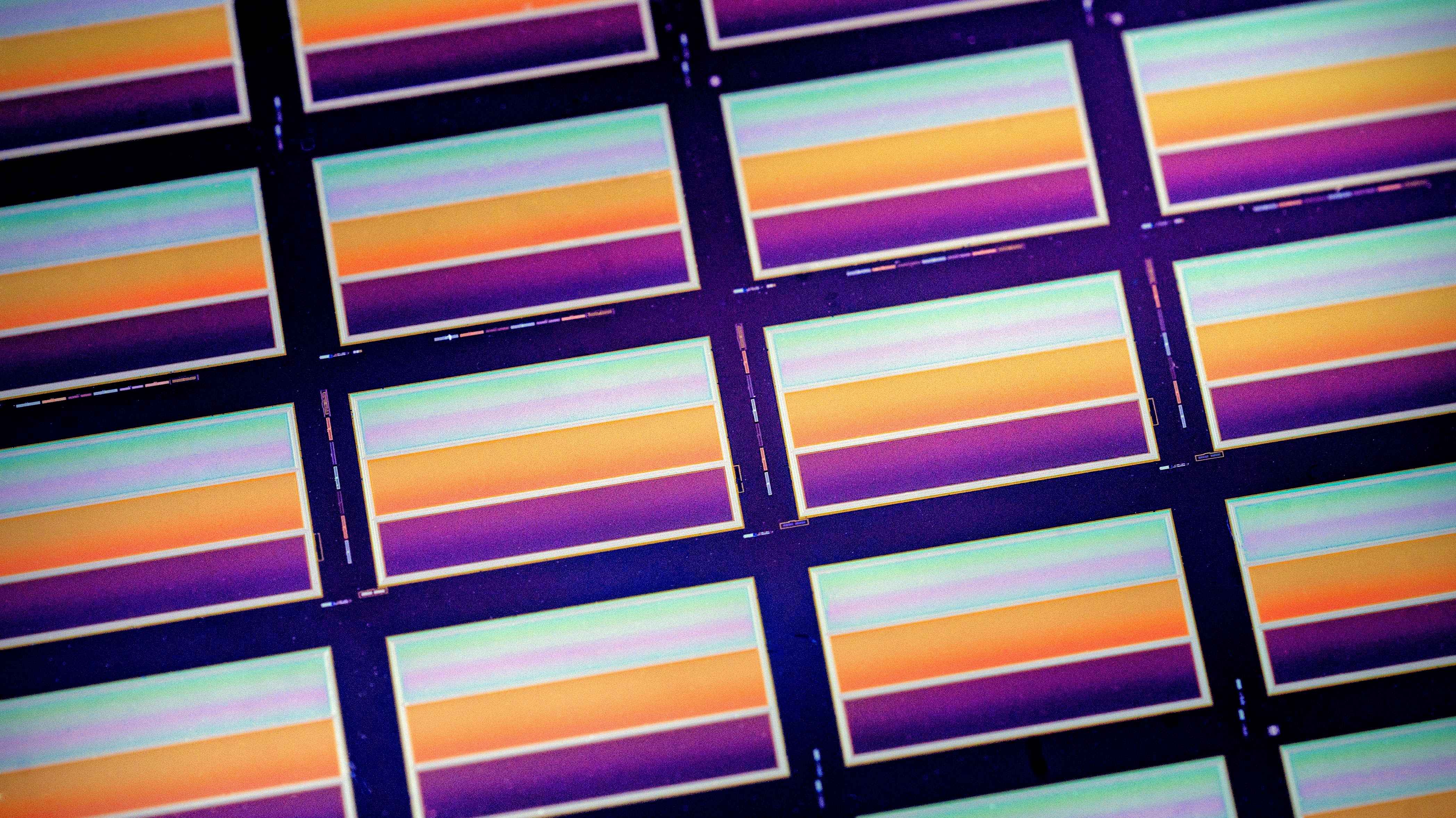
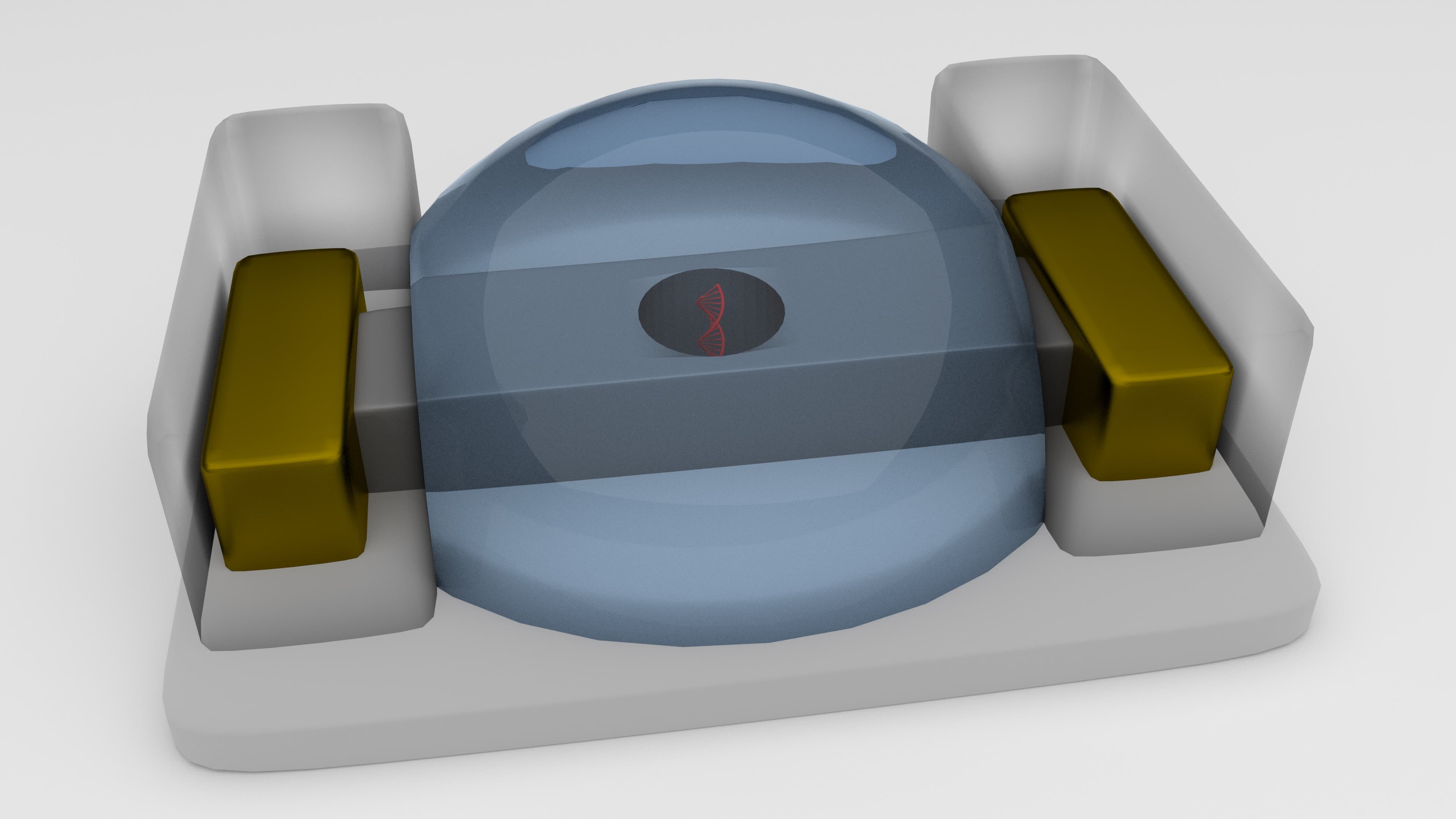
At 70% transparency in the visible region, the new prototype is the most transparent large-area optical fingerprint sensor yet. It is based on a proven combination of organic photodiodes (OPD), thin-film barrier and oxide thin-film transistors (TFTs) pioneered by Holst Centre. To achieve the high transparency, the team uses photolithography to pattern the photodiode layer within each pixel, creating microscopic islands of photosensitive material.
The transparent sensor offers high resolution and dynamic range with a low dark current, ensuring excellent sensitivity even in low light conditions. It can also be produced in large sizes for example to read palmprints or 4 fingerprints at once. This combination of size and performance enables compliance with FAP 60, the FBI’s most-stringent certification category.
It also allows the sensor to work as a document scanner, for example allowing a single system to read passports and fingerprints while also providing user guidance. Moreover, the new sensor can be used in combination with the highly transparent capacitive touch panels commonly used in LCD screens, enabling simultaneous touch and biometric functionality.
“Integrating biometric sensors into displays allows the display to give people better guidance on how to use the system and exactly where to put their hand. This would make identification, for example at customs, more reliable and much faster. Our patterned pixel design ensures high transparency and is completely compatible with existing flat-panel display production processes, making integration with widely used LCD displays both technically feasible and cost effective,” said Hylke Akkerman, Program Manager at Holst Centre.
As with Holst Centre’s previous fingerprint sensors, the transparent sensor is also capable of detecting a heartbeat while reading a fingerprint for liveness detection. Changes to the photodiode chemistry would allow the sensor to work in the near infrared to detect the pattern of veins in the hand, offering additional ways to verify a person’s identity.
Holst Centre will be unveiling the transparent sensor technology in a demonstrator with an active area of 92.4 x 110.9 mm2. The demonstrator can be seen in the Innovation Show (I-zone) at the Society for Information Display’s Display Week 2019 (San Jose, California, May 12 – 19) and imec’s FutureSummits (Antwerp, Belgium, May 14 – 15).
Holst Centre will also be showing three further fingerprint innovations at Display Week 2019. These include a high-resolution sensor integrated under a display using Holst Centre’s proprietary collimator technology as well as an in-display sensor concept that uses photolithography patterning to integrate OLED and OPD pixels side-by-side. This latter approach could allow 500 ppi fingerprint scanners to be integrated into ultra-high resolution display arrays such as single AMOLED modules with multiple functionalities. On the design side, Holst Centre will demonstrate integrated readout electronics for on-display-panel fingerprint detection.
“Integrating microscopic photodetectors within AMOLED arrays adds light sensitivity to display pixels. Through photolithography patterning, we envision ultra-high resolution arrays of OLEDs and OPD that maximize the usage of the active area. At the same time, in-panel readout blocks could facilitate further scaling of fingerprint scanners for a more-efficient user interface,” adds Pawel Malinowski, Program Manager at imec.
Holst Centre
Judith Tesser
040 40 20 400
Holst Centre
High Tech Campus 31
5656 AE Eindhoven
Published on:
13 May 2019

