Co-integration of large-scale photonic and electronic circuits for programmable photonics
Gent | More than two weeks ago
Bring complex photonic chips and driver electronics together to enable large programmable photonic circuits for accelerators, quantum photonics and general-purpose applications.
In this research, we will look into efficient integration strategies to bring photonics and electronics together to realize large-scale programmable photonic chips.
Programmable photonic circuits are a new class of photonic chip where the flow of light can be controlled by electrical signals, and eventually through software. While they perform very different functions compared to electronics, their use can be compared to an electronic field-programmable gate array (FPGA): through a software interface, the hardware is reconfigured to route signals along specific paths.
Programmable photonic circuit require a lot of electronically addressable actuators, as well as many photodetector readouts. This requires a large count of connections between the photonic chip and its driver electronics, and at the same time the photonic chip might also needs optical and high-speed RF interfaces. This requires new integration strategies to bring all these elements together, combining different expertises within imec. The co-integration strategies for large-scale circuits (with many driver channels operating at low speed) are particularly driven by the Photonics Research Group (PRG) and Center for Microsystems Technology (CMST) located in Ghent, but there is a strong interaction with the IDlab electronics design group (also in Ghent) and the Silicon Photonics team (in Leuven).
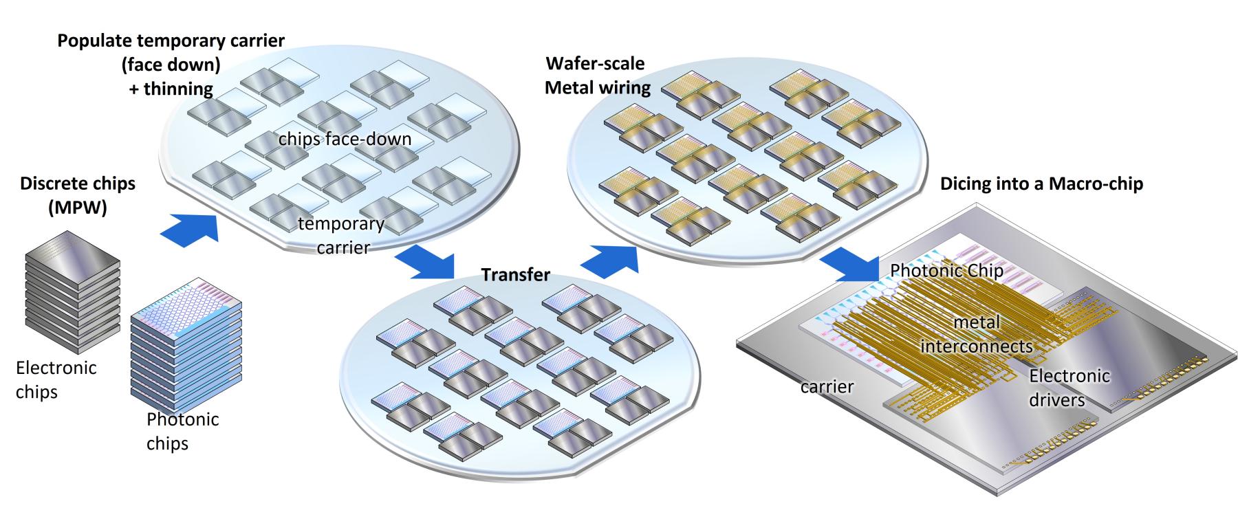
Today, most simple photonic chip assemblies use wirebonding, but this is limited to a small number of channels at the edge of the chip. Flip-chipping, microbumps and micropillars provide higher densities, but complicate the access to the optical ports on the chip. In this work, we will explore different mechanisms to integrate photonics with electronics, such as wafer reconstitution, where photonic and electronic chips are placed side by side and then interconnected with an additional wiring layer. Alternative methods include backside addressing where the photonics is placed on top of the electronic drivers.
The goal of this exploratory work is to identify promising integration strategies that will allow an order of magnitude increase in wiring density in a cost-effective and scalable way.
This will be applied to actual programmable photonic chips. This work can start from chips already developed in the Photonics Research Group, but also using high-speed driver chips developed by the IDlab design team. As the techniques improve, a new generation of chips can be designed to test the scaling potential. The integration will build on techniques developed at CMST for accurate chip placement, adaptive definition of additional wiring layers, and optical fiber attachment. The assembled chips will then be characterized in the optical labs of the photonics research group and high-speed RF labs of IDlab.
This work requires a good affinity with technological processes, as it combines photonic and electronics design, clean room fabrication processes and optical/electrical characterization.
Required background: Electronics, Photonics
Type of work: Fabrication, Circuit Design, Testing
Supervisor: Geert Van Steenberge
Co-supervisor: Wim Bogaerts
Daily advisor: Geert Van Steenberge
The reference code for this position is 2024-136. Mention this reference code on your application form.