Silicon nitride photonic integrated circuits prototyping and small volume production
Integrated photonics based on silicon nitride (SiN) opens a world of applications that use visible and near-infrared light. Seize the opportunity to innovate in this field through imec’s affordable multi-project-wafer (MPW) service.
SiN is an emerging and highly promising material for integrated photonics. The material is:
- transparent for visible and near-infrared wavelengths – which makes it possible to make SiN waveguides with very low propagation loss for applications in healthcare, sensing, imaging, LiDAR, quantum computing, ...
- widely used in semiconductor device fabrications – which makes it highly compatible with CMOS technology.
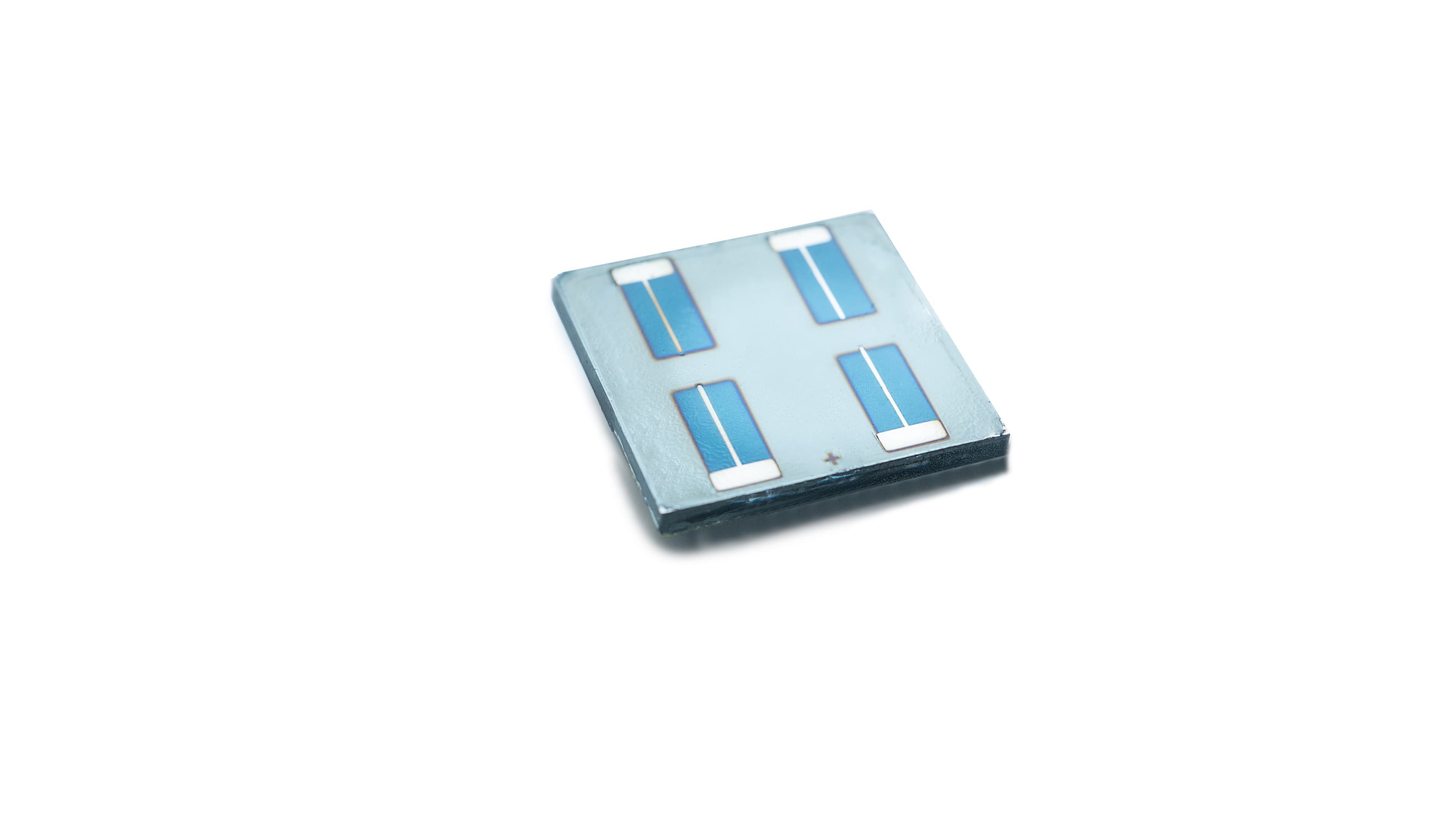
Imec’s SiN photonics platform is based on 180-nm process technology on 200-mm wafers. The deposition of SiN happens through low-temperature plasma-enhanced chemical vapor deposition (PECVD). This method allows highly reproducible and CMOS-compatible fabrication of compact SiN photonic integrated circuits.
This platform is now available for prototyping and low-volume production through imec’s SiN photonics multi-project wafer (MPW) service.
Affordable platform for photonic integrated circuits
Imec’s SiN photonics platform offers the following processing modules:
|
Modules |
Description |
Enabled devices |
|
|
2 SiN thickness flavors |
SiN waveguide layers in 2 stacks: 150 nm (BioPIX150) |
2 flavors optimized for wavelengths 300 – 1000 nm |
|
|
2 SiN patterning steps each |
2 etch depths for each flavor: 150 & 300 nm |
strip/rib waveguides, shallow/deep gratings |
|
|
Clad oxide removal |
Exposure of waveguides for sensing by removing local clad SiO2 |
micro-channels for evanescent sensing |
|
|
Metal heater |
TiN metal lines for resistive heating |
thermo-optic tuners/modulators |
|
|
Metal interconnect |
Al metal lines and pads for interconnects |
interconnects, probe/bond –pads |
|
|
Deep trench |
Deep trench to expose edge coupler facets |
edge couplers |
|
The process-design-kit (PDK) is available for the photonics design software of Luceda Photonics and Synopsys. Its ever expanding library of photonic component designs, developed and validated by EU project PIX4life, further lowers the barrier for designing.
Photonic integrated circuits: from low- to mid-volume production
Do you want to fabricate SiN-PICs in small quantity for prototyping? Then an MPW run is the preferred route for you. By sharing your photomasking and processing costs with other designers.
MPWs yield 20 – 40 dies fabricated on a standard stack. Find out more about the technology, the pricing and the schedule of upcoming runs on the Europractice website.
Do you want to fabricate SiN-PICs in low- or mid-volume with some customization? Then contact us for a dedicated run. Dedicated runs yield 15 full wafers and allow you some degree of customization.


