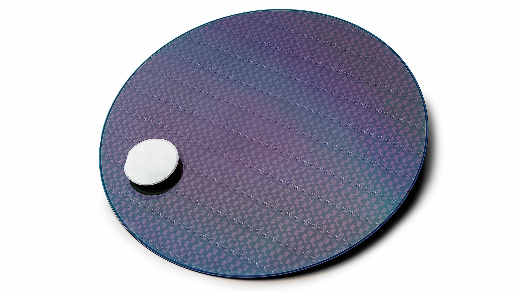
While first commercial 5G wireless networks are going live, imec prepares the next generation mobile handsets – for 5G and beyond-5G applications. More specifically, the team is looking into improving front-end modules by using CMOS-compatible III-V technologies. These front ends will operate at mm-wave frequencies, and will be compact, powerful, cost and energy efficient. Nadine Collaert, program director at imec, sheds light on the technologies that imec is developing and presents first functional devices.
5G to challenge mobile handsets
The fifth generation of mobile networks is expected to take the Internet of Things to a higher level. It will enable extreme mobile broadband, with low latencies and data rates exceeding 10Gbps. With these properties, 5G will underpin the technologies of the next era, from self-driving cars and machine-to-machine communication to smart cities and artificial intelligence.
In 2019, we have seen first commercial 5G wireless networks going live. In this first phase of 5G deployment, wireless communication is mainly supported by the sub-6GHz radio frequency (RF) bands. However, spectrum scarcity within these bands is pushing operating frequencies towards mm-wave bands, with 28-39GHz as the next generation. The introduction of these mm-wave frequencies will have a significant impact on the overall 5G network infrastructure, including base stations and small cells as well as user equipment. For mobile handsets such as smartphones, this translates into increasingly complex front-end modules. These front-end modules send the signals to and from the antenna, using power amplifiers, switches and filters as their main building blocks.
Figure 1: Schematic representation of the increased RF-front-end-module complexity with every generation of mobile communication.
To be able to operate at mm-wave frequencies, the RF front-end modules will have to combine high speed with high output power. In addition, their implementation into battery-powered mobile handsets puts high demands on their form factor, and on their cost and power efficiency. These requirements will especially impact the transmit side of the future RF front-end module.
Today, this module is made up of various technologies, including high-speed GaAs-based heterojunction bipolar transistors (HBTs, typically fabricated on small, expensive GaAs substrates) for making the power amplifiers, and RF-silicon-on-insulator (RF-SOI) for making the RF switches. These components are fabricated and packaged separately, and then later assembled on the same carrier substrate. Innovative solutions will be required to reduce their form factor and cost and to increase their speed and power output.
Key solution: co-integration
An attractive approach to reducing form factor and cost is co-integrating the miscellaneous components of the RF front end in one Si-CMOS-compatible technology. Ultimately, these components can then be co-integrated with other components of the radio communication chip, such as control circuitry and ADCs/DACs. Besides an improved cost and form factor, co-integration is expected to improve the energy efficiency of the overall circuit.
Early 2018, imec set up an Industrial Affiliation Program to reach this goal. In a first phase, a CMOS-compatible III-V-on-Si technology is being developed for making high-speed devices with high output power. In a second phase, the imec team will delve into the possibility of co-integrating these devices with other CMOS-based components, either through monolithic or 2D integration (with the Si devices and the III-V devices in the same plane), or by using 2.5D or 3D integration technologies.
Identifying the right devices
The team is investigating which (CMOS-compatible) devices and device architectures can deliver the desired performance characteristics. Two different routes are being explored, each of them to enable a different range of operating frequencies.
As a first route, GaN-based devices are being examined for the lower mm-wave frequencies. Devices based on this III-V wide-bandgap material have high power handling capabilities and are therefore very promising for making power amplifiers with high output power. Today, these devices are being used for power electronics applications and are used for base stations, where they typically work at high operating voltages above 28V. To be useful for mobile handsets, the operating voltage must be lowered significantly (below 5V), and the buffer layers must be made RF compatible, minimizing RF losses. Other challenges include their integration into Si and finding a suitable architecture that can deliver high RF operating speeds. To help achieve this goal, the imec team can rely on its long-standing expertise in GaN-on-Si technology originally developed for power electronics applications.
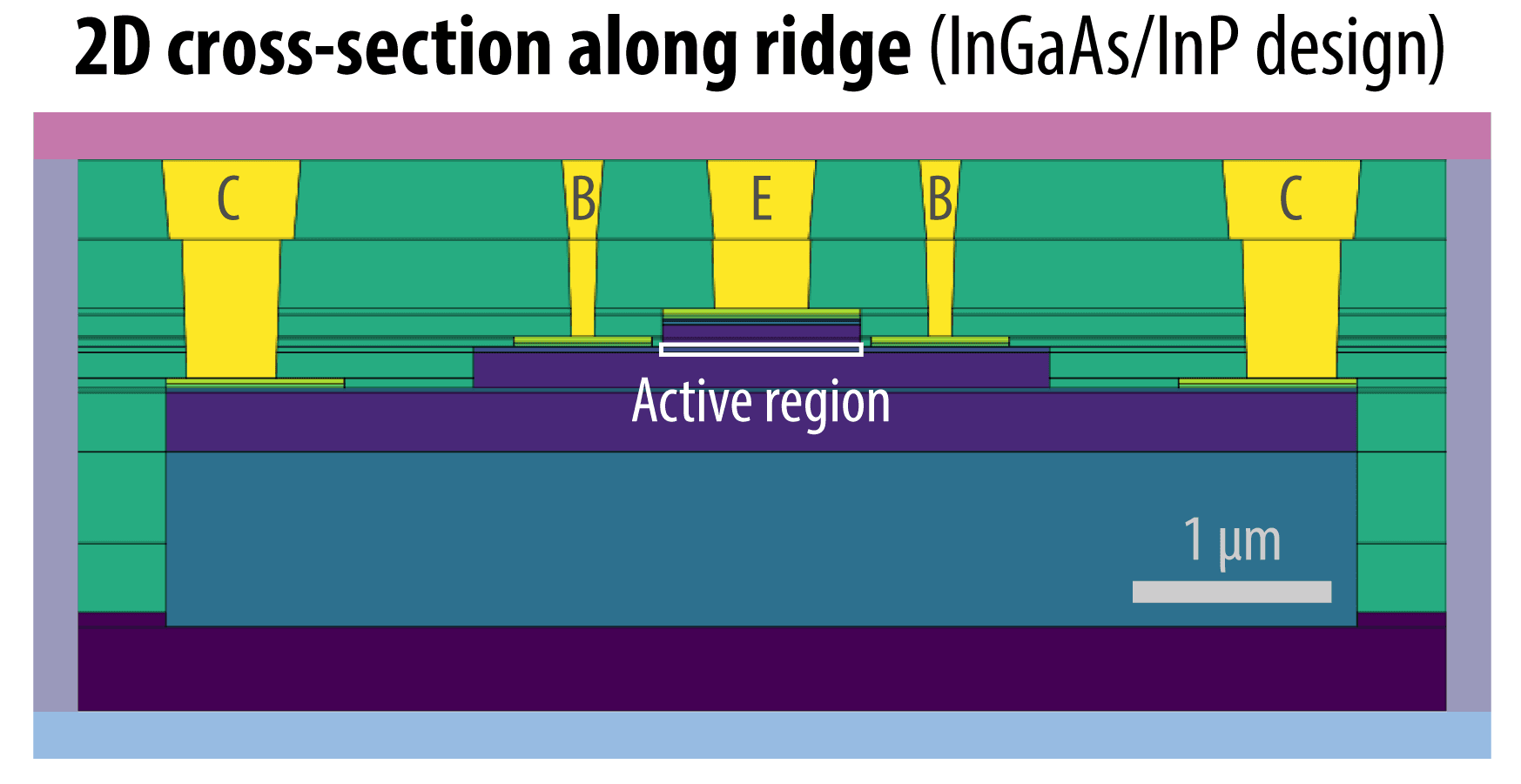
The second route focuses on integrating InP-based devices on Si, thereby leveraging imec’s expertise on III-V-on-300mm Si – developed in the context of CMOS scaling. In a first instance, the team is looking at HBT devices which is a type of bipolar junction transistor (BJT) that uses different semiconductor materials for the emitter and base regions, creating a heterojunction. High-speed capabilities of GaAs-based HBTs with InGaP incorporated into the emitter have already been demonstrated. Higher mobilities can be expected from InGaAs-based or InP-based devices, paving the way towards mm-wave operation far beyond 28-39GHz and already tackling the 6G challenges.
Comparing different GaN-on-Si device architectures for high-frequency operation
As a first route, the imec researchers integrated GaN-based devices with an AlGaN barrier on 200mm Si using Au-free processing in standard Si CMOS tools. To identify the most promising scalable architecture for high-frequency operation, the team compared three different device architectures. They were looking for a device that exhibits positive as well as with negative threshold voltages (VT), as to ensure flexibility in designing circuits.
A first class of devices are GaN HEMT devices. These are depletion mode (or d-mode, normally-on) devices that implement a Schottky metal gate (without high-k oxide) and have a negative threshold voltage (VT). At the other end of the ‘spectrum’ are GaN-based MOSFET ‘normally-off’ devices, exhibiting a positive VT. This positive VT operation, comes at the expense of performance as the AlGaN barrier is etched away in the channel area prior to gate stack deposition, leading to a removal of the two-dimensional high mobility electron gas (2DEG). ‘In between’ HEMT and MOSFET devices are MISHEMT (or MOSHEMT) devices that combine the best of both worlds. It is expected that the threshold voltage of these devices can be tuned between positive and negative by optimizing the thickness of the AlGaN barrier.
Figure 2: Different GaN-based device architectures: HEMT, MISHEMT and MOSFET (presented at 2019 IEDM).
Figure 3: Cross-sectional schematic and transmission electron microscopy (TEM) picture of a fully processed device (presented at 2019 IEDM).
The imec team showed that MISHEMT devices outperform the other device types in terms of scalability and noise performance for high-frequency operation. These MISHEMTs also show the highest mobility (i.e., field-effect mobility larger than 2000cm2/V.s). Peak cut-off frequencies of fT/fmax = 46/38 were obtained for 300nm gate lengths and for a drain bias condition of only 4V. This fT/fmax, a measure for the intrinsic speed of the device, ensures operation in the sub-6GHz bands.
Figure 4: GaN/AlGaN devices on 200mm Si: measured cut-off frequencies of the current gain (fT) and of the unilateral power gain (fmax) at VDS=2.5V and 4V (presented at 2019 IEDM).
To optimize the device for higher operating frequencies, further downscaling of the gate length of the device is needed – as this will benefit a higher fT/fmax. First results with AlInN as a barrier material show the potential to further improve performance by increasing the 2DEG properties, and hence increase the operating frequency of the GaN-based MISHEMT device.
First functional GaAs-based HBT devices on Si: a new growth approach
Growing III-V materials such as GaAs on Si usually goes along with the introduction of defects – mainly threading dislocations – due to the large lattice mismatch between the materials. These defects induce leakage currents, which can dramatically deteriorate device performance. One way to lower the defect density is by growing thick (1-10µm) strain relaxed buffer layers (e.g. SiGe or a complex III-V metamorphic stack) on top of which the III-V active layers can be grown.
Imec proposes a different approach that eliminates the need for implementing additional thick buffer layers. The new process combines aspect ratio trapping (ART) with material overgrowth – also known as imec’s unique nano-ridge engineering (NRE) process. With ART, a trench is made into the Si substrate, which is then filled with III-V material. Most of the defects generated by the lattice mismatch are now confined in the bottom of this high-aspect-ratio trench. This ensures the growth of material with low threading dislocation density out of the narrow trench. At the same time, this overgrowth allows to widen the nano-ridge, resulting in a large box-like shape. This material with low defectivity can then be used for making the device stack.
Figure 5: Description of the NRE approach for hybrid III-V/CMOS integration on 300mm Si: (a) nano-trench formation; defects are trapped in the narrow trench region; (b) HBT stack growth using NRE and (c) different layout options for HBT device integration (presented at 2019 IEDM).
By using this approach, imec has recently demonstrated first functional GaAs-based HBTs grown on 300mm Si, as a first stepping-stone towards the enablement of InGaAs-based devices. The density of threading dislocations at the surface of the GaAs nano-ridges was shown to be below 3x106cm-2. The quality of the layer interfaces was found to be similar as for layers grown on GaAs substrates. GaAs/InGaP HBT devices were subsequently fabricated. The performance of these devices outperformed that of a reference device that incorporates a thick strain relaxed buffer layer on top of Si.
This demonstration shows the potential for enabling a hybrid III-V/CMOS technology for 5G and mm-wave applications. To achieve higher operating speeds, imec sees an extension towards higher-mobility InP-based HBTs as the way forward.
Figure 6: Comparison of electrical characterization (Gummel plots) of the devices fabricated in this work with that of reference devices [1] with strain relaxed buffer layers (presented at IEDM 2019). [1] C. Heidelberger et al., Journal of Applied Physics 123, 161532 (2018)
In summary
The next-generation 5G mobile handsets need small and cost- and energy-efficient front-end modules that can operate at higher speeds and deliver more output power than the first-generation front ends. Imec sees a heterogeneous III-V/Si-CMOS technology as the way forward, ultimately enabling the co-integration with other components of the radio chip. Two routes are being investigated: (1) GaN-on-Si for low mm-wave frequencies and (2) InP-based HBTs-on-Si for operating frequencies above 100GHz. For both technologies, imec demonstrated first functional devices and identified ways to further enhance their operating frequency. This paves the way towards the next-generation RF front ends for 5G mobile handset applications and even beyond. The developed technologies will be useful for other applications, in need of high data rates as well, including VR/AR.
This article was published in Microwave Journal, Jan. 2020.
Want to know more?
- Want to read more about imec enabling beyond-5G? The results presented in this work have been summarized in a press release.
- Read the article on the launch of imec’s highspeed analog/RF program in imec magazine.
- More details of this work can be found in two IEDM papers: (1) ‘First demonstration of IIIV HBTs on 300mm Si substrates using nano-ridge engineering’ by A. Vais et al.; (2) ‘CMOS-compatible GaN-based devices on 200mm-Si for RF applications: integration and performance’ by U. Peralagu et al. Both papers can be requested via our contact form.

Nadine Collaert is program director at imec and responsible for the High-speed analog/RF program. She received an M.S. and Ph.D. degree in electrical engineering from the ESAT Department, KU Leuven, Belgium, in 1995 and 2000, respectively. Since then, she has been involved in the theory, design and technology of FinFET devices, emerging memory devices, transducers for biomedical applications and the heterogeneous integration of new materials with Si.
Published on:
9 January 2020


